Part 7 of 7 in the Hardware hacking series. Part 1: updating the firmware on a Pinecil V2. Part 2: the bench I work on. Part 3: using my 5V FTDI cable on 3.3V UARTs. Part 4: finding the UART console on a router I own. Part 5: reading SPI flash without wrecking it. Part 6: decoding I2C and SPI with sigrok.
UART gives you a console, SPI flash gives you the firmware image, and JTAG or SWD gives you the CPU itself. Halt it, read registers, step through code, read and write memory, reflash, all on a part that has not been locked. That is why the debug port is the most powerful interface on a board and why vendors spend effort making it go away in production.
This is the one part of the series where I own less than the topic needs. I have no dedicated debug probe, so this part is about understanding the interface and how defenders lock it, not a walkthrough of attacking a device. Everything here applies only to hardware you own or are authorised to test. Ownership does not switch off copyright or anti-circumvention law, so check yours before you bypass read protection on anything.
What the two interfaces are
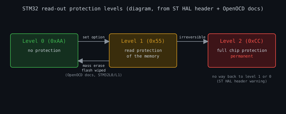
The diagram above summarises the protection levels described below; it is a diagram I drew, not a screenshot.
JTAG is the old one. It uses four signals, TCK (clock), TMS (mode select), TDI (data in) and TDO (data out), plus an optional active-low reset for the test logic, usually written nTRST. Devices sit in a chain, and OpenOCD’s documentation notes that JTAG also supports boundary scan testing.
SWD is the ARM-specific alternative. The OpenOCD manual describes it as using fewer signal wires than JTAG: SWDIO and SWCLK, plus ground and usually a reset line. It has no boundary scan. Some processors support both.
The pin counts matter for defenders because they decide how easy it is to find the port on an unmarked board. Here is the number of ways to assign the data signals if you have a row of n candidate pads and no silkscreen. These are my own permutation counts, not a vendor figure, and they ignore the ground, reset and reference-voltage pads on the same header:
pads   JTAG (TCK,TMS,TDI,TDO)   SWD (SWDIO,SWCLK)
  6            360                    30
  8           1680                    56
 10           5040                    90
 12          11880                   132
 16          43680                   240
Few people try them by hand, and pin-finding tools exist for exactly this. Those tools drive the pads, and an unknown pad can be a supply rail, so set the tool to the target’s measured logic level first and never use one on a mains-connected board. I treat unpopulated pads as obscurity, not as a control.
What the software side looks like
OpenOCD is the open source tool that sits between a debug adapter and GDB. The adapter list in my capture comes from the real 0.12.0 package on Ubuntu 24.04. One entry is ft232r, which drives an FT232R in bitbang mode, so in principle my cable could act as a crude JTAG adapter. I have not tried it and will not. The seller describes the cable as 5V logic (I confirm by measuring TXD at idle, as in part 3), and most debug ports are 3.3V or lower.
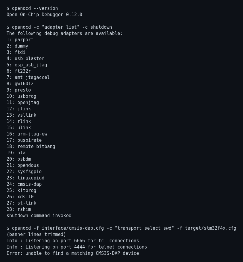
Real terminal output from OpenOCD 0.12.0 in a throwaway container: the list of built-in debug adapters, then a run with no probe attached.
The second command, run with no probe attached, shows a failed first attempt: OpenOCD opens its TCL and telnet ports, then stops with “unable to find a matching CMSIS-DAP device”. Both outputs are real, from a throwaway container, and prove nothing about any chip.
How vendors lock it
Most microcontroller vendors have some version of the same idea: a setting in non-volatile memory that tells the chip to refuse debug access, or to refuse it unless the flash is erased first.
STMicroelectronics calls it read-out protection. In the HAL header for the STM32F4 family, level 0 is 0xAA (no protection), level 1 is 0x55 (read protection of the memory) and level 2 is 0xCC (full chip protection). The same header carries the warning that once level 2 is set it is no longer possible to go back to level 1 or 0. OpenOCD’s documentation for the STM32L0/L1 driver says mass erase is the only way to unlock a protected flash, unless the level is 2, which cannot be unlocked at all. On those parts, dropping from level 1 to level 0 wipes the flash, so the attacker gets the chip back but not the firmware. That is the design intent. As the next section shows, it did not always hold.
Espressif does it with eFuses. The ESP-IDF documentation says that when secure boot is enabled, JTAG debugging is disabled via eFuse, and the bootloader sets that on first boot at the same time it enables secure boot. Flash encryption disables it by default too. The eFuse names vary by chip (DIS_PAD_JTAG and DIS_USB_JTAG on some, HARD_DIS_JTAG on the ESP32-S2). eFuses are one-time programmable, so the hard-disable ones are a one-way door too. Run your first flash-encryption experiments on a board you can afford to lose.
Locks that fail
A protection bit is only as good as the silicon that enforces it. Two cases I can point to with sources.
Obermaier and Tatschner at Fraunhofer AISEC presented “Shedding too much Light on a Microcontroller’s Firmware Protection” at USENIX WOOT 2017. They looked at the STM32F0 and found three weaknesses: a common configuration that gave low protection and could be exploited with a cold-boot approach, a design weakness that let the protection level be downgraded, and a hardware race condition in the debug interface that let them extract read-protected firmware. Each attack needed only low-priced equipment, according to the abstract.
CVE-2020-27211 is the nRF52840 case, where Nordic’s flash read-out protection is called APPROTECT. NVD describes it as being bypassable by injecting a fault during the boot phase, with a CVSS 3.1 base score of 5.7 and a physical attack vector. The score is modest for a consumer gadget. For a device holding a fleet-wide secret in flash it is not, which is the point I would make to a product team.
My takeaway for anyone shipping hardware: assume someone with the device in hand eventually gets in, and make sure what they find is worth nothing beyond that one unit. Per-device keys, no shared credentials in firmware, no signing key near the board. The lock buys time. It does not keep a secret.
What I check on my own devices
On a product I am responsible for, “debug port open, same key on every unit” goes in the risk register ahead of most software findings.
If you do connect a debug adapter to a board you own, these rules come from the earlier parts and I follow every one of them:
- Power the target from its own supply, and only one source at a time. Never connect an adapter’s power output to a target that has its own supply, least of all the red 5V wire of a cable like mine. The reference-voltage pin, where the adapter has one, is a sense input and the only power-related pin to wire.
- With the board powered and nothing connected, measure its supply or the header’s reference pad against ground to learn the logic level. Then power down, connect ground first and the signals second, power up, and only then start OpenOCD. Disconnect in the opposite order.
- Power the board down, and disconnect any battery, before moving a lead or soldering a header. Let the iron tip cool before you put it away.
- Do not probe or connect anything to a board that is plugged into mains, or whose supply is mains-connected and non-isolated. A low-voltage output does not make it safe, and bulk capacitors stay charged after you unplug.
- Touch a grounded object first or use a wrist strap, and handle boards by the edges. Do not wear a wrist strap near mains-connected circuits.
- Read the protection settings before you change them, and back up the firmware before you lock anything, because afterwards you cannot. Level 1 on an STM32 can only be removed by a mass erase, level 2 cannot be removed, and ESP32 eFuse burns cannot be undone and can brick the board.
That closes the series. Measure first, read before you write, and back up the thing you cannot replace.