Part 5 of 7 in the Hardware hacking series. Part 1: updating the firmware on a Pinecil V2. Part 2: the bench I work on. Part 3: using my 5V FTDI cable on 3.3V UARTs. Part 4: finding the UART console on a router I own.
The flash chip is where a device keeps its firmware, its configuration and often the secrets that were supposed to stay secret. On most external SPI flash, anyone who can read the chip gets whatever is stored in the clear, no exploit needed. I want to know what comes out of my own devices, and I want to read it without killing the board.
Everything here is for hardware I own, on boards that run from a low-voltage adapter or a battery. I never open or probe anything with mains-voltage circuitry inside, and never connect anything to a board that is plugged into the wall. If I can’t tell what powers it, I leave it alone. Before handling a board I touch an earthed metal object or wear a wrist strap, because flash chips are ESD sensitive.
Read the datasheet for the exact chip first
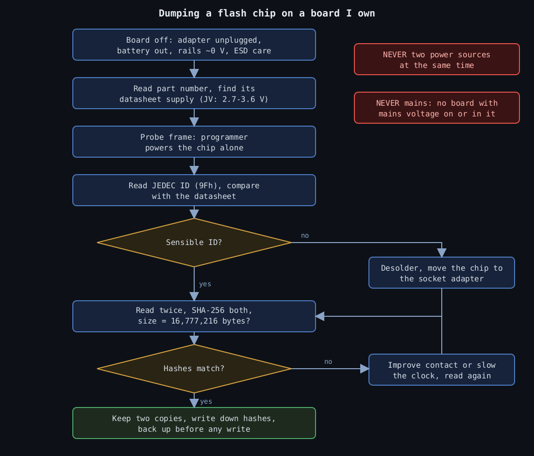
The flowchart above is a diagram I drew. It is the order I work in, and the two red warnings apply at every step.
I’ll use the Winbond W25Q128JV (datasheet Revision F, March 2018). In the 8-pin SOIC package the pins are 1 /CS, 2 DO (IO1), 3 /WP (IO2), 4 GND, 5 DI (IO0), 6 CLK, 7 /HOLD (IO3, labelled “Hold or Reset” in the datasheet) and 8 VCC. Pin 1 sits next to the dot. Every other part gets its own datasheet check.
The supply range is 2.7V to 3.6V (section 9.2), with the lower part allowed only at lower maximum clock speeds. The absolute maximum for VCC is 4.6V, and no pin may go above VCC plus 0.4V (section 9.1). That is why a 5V signal has no business near these pins. If the marking says a different family member, a lower-voltage one for instance, I read that datasheet before powering it.
The cheapest sanity check is the JEDEC ID. Instruction 9Fh returns a manufacturer byte (EFh for Winbond) and two device bytes: 40h 18h for the W25Q128JV-IQ/JQ, 70h 18h for the -IM/JM variants. A sensible ID means contact, supply and wiring are probably fine for those few bytes, which says nothing yet about a full read. All zeros or all ones means I stop and fix the contact.
In-circuit reads and why they fail
When I can’t or don’t want to desolder, I use the probe frame, four spring pens that press on the chip’s legs. It’s quick and leaves the board as it was. It also fails often.
The chip is not alone on the bus. The SoC is usually wired to the same pins. If it’s unpowered, current can leak through its protection diodes from whatever the programmer drives. If it’s powered, it may read the flash while I do. The result is a garbled ID, or a read that looks fine and is subtly wrong.
The programmer’s supply may also feed the board’s whole 3.3V rail, and the board can power itself backwards through the chip’s lines. A faint LED glow on a board that should be off is the symptom, and on glow, heat or a smell I disconnect and go to the socket.
One rule I never bend: exactly one power source at a time. The board’s adapter is unplugged and any battery is out, and a lithium cell never stays in a board I’m clipping onto. I wait until a meter shows the rails near 0V, since capacitors hold charge. Before clipping on I check pin 1 against the clip’s marked wire, and I measure the programmer’s output with a meter, because a cheap programmer can put 5V on its data lines, which is fatal to a 3.3V chip.
Read twice, then compare
I read the chip at least twice and hash both files. The terminal below shows the routine with flashrom. There is no real chip in it. I used flashrom’s dummy programmer, which emulates a W25Q128FV (an older family member than the JV above) from a 16 MiB file of random data I generated, so it is real software on a synthetic target, not a hardware capture.
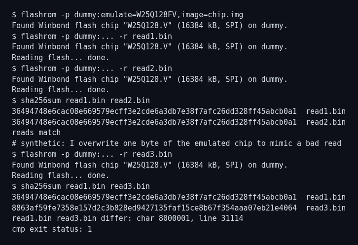
The screenshot is real flashrom output on the emulated chip. I trimmed flashrom’s banner and its “untested operations” notice, and nothing else.
The first two reads give the same SHA-256. For the third I overwrote one byte of the emulated chip to mimic a bad contact, and the hash changes completely while cmp names the byte. A mismatch is a signal. A match is not proof.
sha256sum read1.bin read2.bin
cmp read1.bin read2.bin && echo "reads match"
ls -l read1.bin
A bad contact can fail identically twice, so I also check that the size equals the capacity (128 Mbit is 16,777,216 bytes) and that the headers and strings look sane. A slow clock helps. At 1 MHz a full read is at least 134 seconds of bit time, at 8 MHz about 17. My programmer is the XGecu T48 with its Windows-only Xgpro software. I didn’t run it for this post, so there’s no screenshot, and I’m not claiming flashrom supports it.
Desoldering and the socket
If the in-circuit read won’t settle, I move the chip to the T48’s socket adapter. That removes everything else from the bus and is riskier for the board. Hot air or an iron can lift pads or cook the chip if I rush. The tool and board stay hot after switch-off, so I park the iron, let things cool, use a fan for the flux fumes and wear eye protection. Hot air blows small parts away, and any lithium cell comes out before I heat anything. I photograph the pin 1 marking first. In the software I select the exact part number and compare the supply voltage it shows against the datasheet. A wrong selection can put 3.3V on a 1.8V part. Bare chips go in anti-static packaging.
Back up before any write
A read changes nothing. A write or erase can brick the device, and the dump is the only way back. So two matching reads, hashes written down, files copied elsewhere, and only then do I think about writing. Per-device data is the trap. Many routers keep their MAC address and radio calibration in flash, and a stock image written over it loses that for good.
The chip’s write protection is weaker than people assume. Array protection comes from the BP, TB and CMP bits in the status register. SRP, SRL and the /WP pin only decide whether those bits can be changed, and /WP stops acting as a protect pin when quad mode turns it into IO2. At the factory default (SRL=0, SRP=0) the status register can be rewritten after a Write Enable, so anyone on the bus can undo the protection. SRP=1 with /WP held low locks it in hardware. SRL=1 locks it until the next power cycle. A separate one-time-programmable mode locks it permanently. None of it stops a read. Write protection is about integrity, not secrecy.
What a defender does about it
I assume anyone with ten minutes and physical access can dump the external flash chip on a board I deploy. The design question is what the dump gives them.
A shared password, a fleet-wide key or a plaintext Wi-Fi passphrase means one stolen device compromises all of them. Secrets should be per-device, and where the hardware allows, held in a secure element or SoC fuses instead of the external chip. Firmware should be signed and checked by a boot ROM the attacker can’t rewrite, so a modified dump doesn’t boot. Anything confidential on flash should be encrypted with a key that doesn’t sit next to it. Otherwise the chip is a USB stick.
Part 6 moves to the logic analyzer, decoding SPI and I2C on a powered board. It is a different setup with its own warnings, ground first and only measured low-voltage lines.
Other parts of the Hardware hacking series: 1, updating the firmware on a Pinecil V2; 2, the bench I work on; 3, using my 5V FTDI cable on 3.3V UARTs; 4, finding the UART console on a router I own; 5, reading SPI flash without wrecking it; 6, decoding I2C and SPI with sigrok (publishes Nov 12); 7, JTAG and SWD basics (publishes Nov 13).
Leave a Reply
You must be logged in to post a comment.